3 Must be wide enough to enclose a contact. The courses are so well structured that attendees can select parts of any lecture that are specifically useful for them.
Ppt
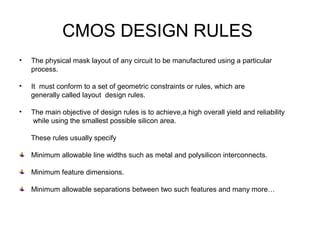
To familiarize the student the student to the basic CMOS layout concepts and the MOSIS scalable CMOS design rules.

. Lambda parameter absolute dimensions micron rules CMOS Process Layers Intra-Layer Design Rules Transistor Layout Vias and. When two or more sticks of different type cross or touch other there is no electrical contact. Width of pMOS should be twice the width of nMOS.
The only constant in VLSI is constant change. Metal-Oxide-Semiconductor Field-Effect Transistor N-type MOS NMOS and P-type MOS PMOS Voltage-controlled switches A MOSFET has four terminals. In a 06 µm process this corresponds to an actual width of 12 µm and a length of 06 µm.
Lambda Based Design Rules. Design rules I The geometric design rules are a contract between the foundry and the designer. Gate source drain and substrate body Complementary MOS CMOS Using two types of MOSFETs to create logic networks NMOS PMOS.
Min feature size and allowable feature specification are stated in terms of absolute dimension in micron. Register for exams Timelines and Guidelines Course Booklet Part 1 Part 2 Part 3 Part 4. The design rules are usually described in two ways.
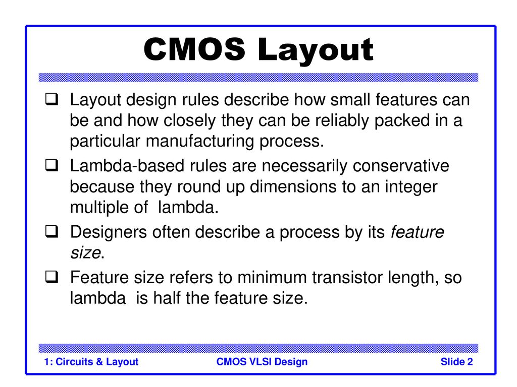
1 Rules for N-well as shown in Figure below. A prose quotation of five or more lines or more than 100 words should be blocked. Specify layout constrains in terms of a single parameter and thus allow linear proportional scaling of all geometrical constrains.
Simple for the designer. The MOSIS rules are scalable λ rules. Diffusion and Tap Width and Space Martin p44 Cypress nwell Diff-tap poly Pdiff Minimum width.
When two or more sticks of the same type cross or touch other that represents electrical contact. Specified in terms of Scalable parameter Design Rule Check DRC essential Spec2Layout2 8. Minimum width 10λ 2.
Layout Design rules Lambda CMOS Layout. Minimum separations minimum and maximum widths overlap rules. Worlds Best PowerPoint Templates - CrystalGraphics offers more PowerPoint templates than anyone else in the world with over 4 million to choose from.
Sketch a 4-input CMOS NAND gate CMOS Gate Design Activity. The USP of the NPTEL courses is its flexibility. Theyll give your presentations a professional memorable appearance - the kind of sophisticated look that.
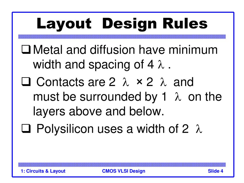
CMOS VLSI Design The rules describe the minimum width to avoid breaks in a line minimum spacing to avoid shorts between lines and minimum overlap to ensure that two layers completely overlap. The Purdue University Online Writing Lab serves writers from around the world and the Purdue University Writing Lab helps writers on Purdues campus. Inverter layout Bring up the Cadence CIW window and create a new library lab7 or open the existing library lab7.
Wells at same potential with spacing 6λ 3. Cross-Section of CMOS Technology Design Rules Interface between designer and process engineer Guidelines for constructing process masks Unit dimension. How to build your own simple CMOS chip CMOS transistors Building logic gates from transistors Transistor layout and fabrication Rest of the course.
I They guarantee that the transfers onto the wafer preserve the topology and geometry of the patterns. Extra electron n-type Group III. This Presentation slides consists of the various design rules associated with layout stick Diagrams with basic CMOS Gates explained.
Download to read offline. Minimum width 3λ 2. Create a new cellview inverter of type layout under the lab7 library.
Wells at same potential 0λ 4. How to build a good CMOS chip 0. Vlsi Design Cmos Layout Ppt Download CMOS recommends blocking two or more lines of.
1 Peak doping concentration needs to be repeatable independent of width or the lateral diffusion 2 Photoresist must have a minimum opening to allow the implant. Design rules based on single parameter λ. Transistor dimensions are often specified by their WidthLength WL ratio.
Winner of the Standing Ovation Award for Best PowerPoint Templates from Presentations Magazine. Design Rules Takes care of manufacturing tolerances Specifies minimum allowed dimensions Line width Spacing between lines on same layer Spacing between lines on different layers Overlap between features where required Diffusion requires higher tolerance. N diff Poly P diff Contacts Metal P Substrate N Well.
To direct and control logic signals in IC design MOSFET. Sketch a 4-input CMOS NOR gate Complementary CMOS Complementary CMOS logic gates nMOS pull-down network pMOS pull-up network aka. Missing electron called hole p-type nMOS Operation Body is commonly tied.
Circuits Layout CMOS VLSI Design Slide 45 Gate Layout qLayout can be very time consuming Design gates to fit together nicely Build a library of standard cells qStandard cell design methodology V DD and GND should abut standard height Adjacent gates should satisfy design rules nMOS at bottom and pMOS at top. The MOSIS design rules are as follows. I These rules are the designers interface to the fabrication process.
Wells of different type spacing 8λ 2 Rules for Active area shown in Figure below. Design Circuits Layout Outline CMOS Gate Design Pass Transistors CMOS Latches Flip-Flops Standard Cell Layouts Stick Diagrams CMOS Gate Design Activity. If contact is needed show explicitly.
Rules for Drawing Stick Diagrams. 26 likes 45577 views. CMOS Mask layout Stick Diagram Mask Notation 11-14 Basic design rules Same N and P alters symmetry L min Wpmos2 Wnmos Width of pMOS should be twice the width of nMOS.
Layout Design rules Lambda Same N and P alters symmetry L min Wpmos2 Wnmos. Introduction Silicon Lattice Transistors are built on a silicon substrate Silicon. For working professionals the lectures are a boon.
Overview Physical principles Combinational logic Sequential logic Datapath Memories Trends Dopants Silicon is a semiconductor Pure silicon has no free carriers and conducts poorly Adding dopants increases the conductivity Group V. Complementary Metal Oxide Semiconductor Fast cheap low power transistors Today. Minimum line width scalable design rules.
Layout and Rules Reasons behind Rules. Minimum spacing 3λ 3.
Cmos Design Rule
Vlsi Design Cmos Layout Ppt Download

Chapter 4 Mos And Cmos Ic Design Ppt Download
Vlsi Design Cmos Layout Ppt Download

Lecture 2 Cmos Vlsi Design Slide 3

Introduction To Cmos Vlsi Design Lecture 1 Circuits Layout Lecture Design Rules Dry Erase Markers
Cmos Vlsi Design Introduction Ppt Video Online Download
Vlsi Design Cmos Layout Ppt Download
0 komentar
Posting Komentar